Listening room
Inside Intel’s race to build chips for an AI-constrained world
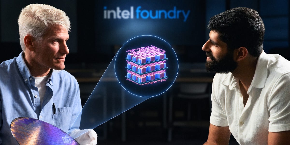
Dwarkesh Patel tours Intel facilities and interviews technical leaders about how advanced chips move from research to high-volume manufacturing. The episode explains gate-all-around transistors, backside power, High-NA EUV, ruthenium wiring, CFETs and hybrid bonding, then connects those technologies to AI-driven capacity constraints. Intel executives argue that equipment supply, yield, scale and execution may matter more than small differences in transistor density. Long-range forecasts and claims about competitors remain interviewees’ views rather than independently verified conclusions.
Editorial summary · Publisher transcript
The takeaways
- New process nodes involve roughly 2,000 manufacturing steps, with yield improved through metrology, failure analysis and tightly managed experiments.
- Intel’s leaders say existing global equipment supplies could support roughly twice, but not ten times, today’s leading-edge wafer output without a much larger upstream ramp.
- Backside power can make High-NA EUV more economically useful for Intel than for some competitors because it relaxes front-side wiring requirements.
- CFETs and other three-dimensional architectures remain research projects whose main obstacles include interconnects, thermal management, aspect ratios and process integration.
- Hybrid bonding is entering volume manufacturing with much denser connections than solder-bump packaging, while chip-to-wafer and wafer-to-wafer approaches serve different architectures.
- Intel’s executives frame catching up with TSMC primarily as a problem of scale, predictable yields, customer-ready process design kits and timely execution.
How a process node becomes manufacturable
Chris Auth describes 14A as the result of more than three years of development and about 2,000 factory steps. Engineers use inline measurements, electrical tests and cross-sections to trace defects to particular parts of the process. The central discipline is balancing innovation against a customer’s required schedule: too many simultaneous changes can produce an impressive technology that arrives too late. Intel says its post-10-nanometer process now uses maturity gates for yield, defects and performance before advancing an idea.
From planar transistors to three-dimensional designs
The episode explains the progression from planar transistors to FinFETs and gate-all-around structures as an effort to control leakage by surrounding the conducting channel more effectively. Gate-all-around required new materials, placeholder layers, high-k insulation and additional thermal and etching challenges. Auth presents modern process research as a broad search across materials, tools and architectures rather than the earlier strategy of repeatedly shrinking an established design.
Why lithography economics depend on the whole architecture
High-NA EUV can print smaller features in fewer passes, but its roughly doubled equipment cost makes the economics application-specific. Intel says backside power frees space for signal wiring, allowing High-NA to provide more value in its design than in TSMC’s current architecture. The tool is therefore presented not as a universal advantage, but as one component whose usefulness depends on wiring, process choices, customer requirements and defect risk.
The foundry transition adds software and customer constraints
Intel’s process design kits translate a manufacturing process into usable rules and capabilities for outside chip designers. Auth acknowledges that Intel’s historically internal manufacturing model did not require the same formal customer-facing PDK discipline. The company says 18A exposed a learning curve, while 14A is intended to launch with a more mature kit. That operational layer matters because a technically capable process is not automatically an accessible foundry service.
Research becomes production through staged simplification
CFET research illustrates why a working laboratory demonstration does not quickly become a phone chip. Engineers use short-loop vehicles to test individual materials, devices and integration problems before combining them into more complex structures. Deep etches, tiny filled spaces, heat removal and vertical interconnects can all fail independently. Kavalieros says a simplified one-on-one CFET can establish feasibility, but thousands of steps must ultimately work together and outperform the existing side-by-side approach.
Packaging is becoming a compute bottleneck
As computation grows faster than the available chip edge for communication, packaging must provide denser and more energy-efficient links. Hybrid bonding removes bulky solder bumps by directly joining copper interconnects, but alignment and defect control complicate manufacturing. Wafer-to-wafer bonding can waste good dies when matching is imperfect; chip-to-wafer bonding can pair tested good dies with known-good positions. Intel expects both methods to remain useful depending on the architecture.
AI demand collides with equipment bottlenecks
Intel CTO Pushkar Ranade says ASML’s EUV supply is only one constraint: once a process is fixed, fabs may depend on particular tools and suppliers throughout the flow. He estimates current equipment could support about twice today’s leading-edge output, not ten times, while AI compute demand has historically grown much faster. The executives argue that more tools, clean-room capacity, power, water and upstream suppliers are all needed, with long lead times limiting expansion before the decade ends.
Scale, capital and the case for rethinking fabs
Ranade describes foundries as unusually scale-sensitive because most fab costs are fixed and yield improvements multiply usable output. He says Intel’s technological gap with TSMC may be small in some dimensions, but scale and predictable execution remain decisive. The closing discussion considers whether AI companies and chipmakers should commit capital and equipment earlier, while also questioning whether today’s clean-room layouts and process assumptions are inherited habits. These proposals are strategic judgments, not demonstrated outcomes.
Context & caveats
- The episode is based partly on interviews with Intel employees and executives, so claims about Intel’s competitiveness, capacity, rivals and future investment reflect company perspectives unless separately established.
- The transcript is publisher-provided and appears complete, but machine-transcript uncertainty may affect some technical names, figures or terminology; consult the original recording for clarification.
Why this made the edition
A complete, detailed publisher transcript combines firsthand fab reporting with attributed interviews covering process-node development, advanced packaging, semiconductor capacity constraints and Intel’s foundry strategy. It offers substantial technical explanation and clearly distinguishes interviewer analysis from executive claims.
Source material